Solid Modeling of a Printed Circuit Board in Ansys Discovery - Lesson 3
In this lesson, you will learn how to create some components of a printed circuit board (PCB) and its enclosure.
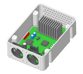
What is a Printed Circuit Board (PCB)?
A PCB is a board that connects different electrical and electronic components through layers of copper and silicon. Many consumer electronics devices use PCBs. Most often, they are assembled in some type of enclosure.
Modeling approach:
Our approach to modeling will begin by analyzing the technical drawing. Download the technical drawing, the model file to start with and other assembly components required for creating this PCB enclosure model here. Once we understand its characteristics, we can outline a plan for completing the PCB enclosure model. With a plan in place, we can begin making the necessary modifications. We will create a capacitor and use it as a template to create several additional parts. The enclosure housing will be modified to improve ventilation, and we will import, as well as create, several additional designs to complete the cooling system.
Check out the videos below to learn the step-by-step process for creating components for the PCB and its enclosure using Discovery.
Part 1 - PCB Components: Capacitor
Part 2 - PCB Housing Ventilation
Part 3 - Fan Housing
Part 4 - Adding Assemblies
Recap:
This printed circuit board modeling session covered several different topics. You learned how to use tools such as Pull (Scale Body), Fill Pattern and Circular Pattern. You then utilized the Shell, Combine and Pull (Revolve) tools to create and modify the geometry of several different components in the assembly. Finally, you assembled components by importing them and applying constraints such as Align.
You are being redirected to our marketplace website to provide you an optimal buying experience. Please refer to our FAQ page for more details. Click the button below to proceed further.